Table of Contents
If you have ever used a phone, a tablet, or a touch screen at the train station, hidden inside is a thin, see-through layer that lets electricity flow while still letting light through. One promising way to make that layer is to weave it from silver nanowires. These are very small metal strands so thin that thousands could fit across a single hair. When they get warm, however, they can change shape, and sometimes that reduces the performance of the whole device. Sometimes it can be turned into an advantage. Our goal was simple. Watch what really happens as these wires heat up and learn how to guide that process so devices last longer and work better.
Why these wires matter?
Traditional transparent conductors based on brittle oxides can crack when bent. Silver and copper nanowire networks bend easily, can be printed over large areas, and are well-suited to flexible electronics. The challenge is heat, but maybe the question arises: why is heat a challenge, and where will it come from?
The answer relies on two main reasons: First, when we produce the nanowire mesh, we need heat to weld the intersections; second, when electrons flow through the nanowire network, the current raises the network’s temperature. When the temperature increases, atoms begin to move along the surface of nanowires, leading to thinning, necking, or even breaking nanowires into tiny pieces, resulting in a loss of electrical conductivity in the network. Understanding the factors that govern the movement of atoms helps us protect the parts we want to keep and deliberately shape the parts we want to change.
What did we watch?
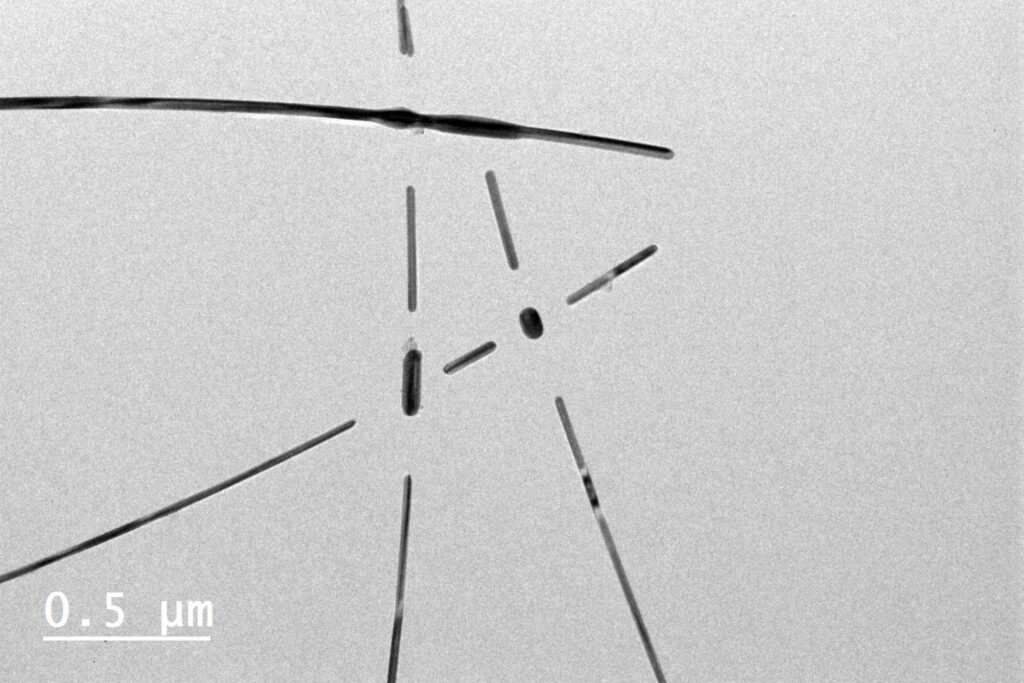
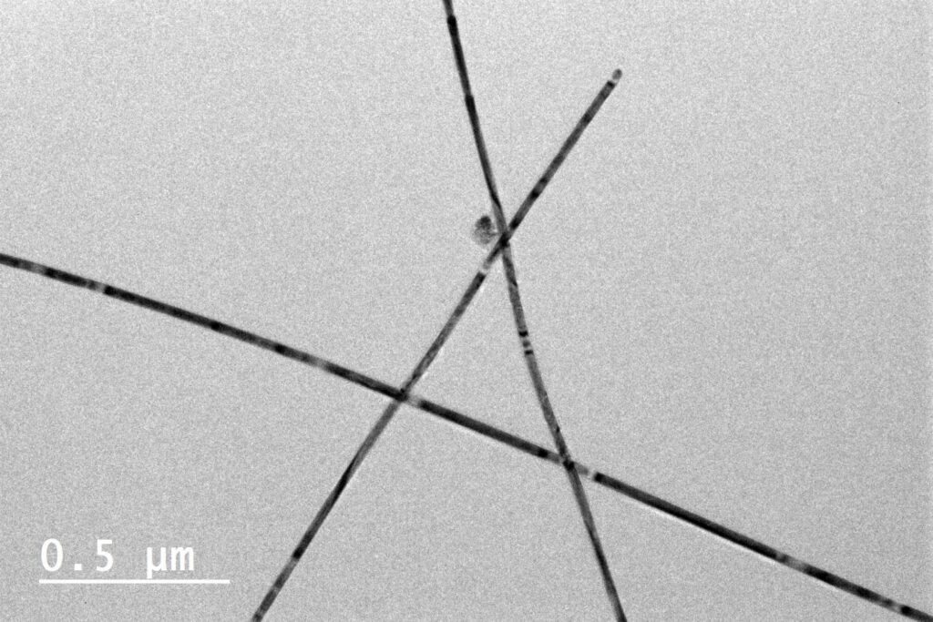
We heated the wires in different environments (vacuum and air). In each environment, we tested different temperatures over heating durations ranging from seconds to hours. We used a silicon wafer to place a solution of nanowires on it to observe changes under the electron microscope. Our electron microscope was equipped with a special heating stage that provides the ability to watch changes during heating inside the electron microscope. Then, we compared the results of heating in different environments and at different temperatures over time. We looked closely in the electron microscope to see which parts changed first. The result was a clear pattern of nanoparticles when we used higher temperatures or let them heat for long periods. Our microscopy results showed that the first sign of change appears at bending areas or at the intersection point (where two or more nanowires cross). By doing a systematic study about the duration of heat treatment for nanowires, we understand there is a relationship between different factors (Temperature, Diameter, and Heating duration). This finding was important for setting these parameters across different applications that use nanowires for varying durations at different working temperatures.
What surprised us?
A very interesting thing is how nanowires can change their morphology due to heating at very low temperatures (e.g., 300 ˚C), even below their melting point (for silver, 960 ˚C). Two details turned out to matter a lot. First, wire thickness. Thinner wires changed faster than thicker ones. For the fragmentation of nanowires in each diameter, there is a critical temperature range. Second, there was an optimal point based on nanowire thickness, heating temperature, and heating duration, which controls the fragmentation of nanowires of different sizes. The crystal structure was also interesting. Longer pieces often retain their initial structure, making these wires strong. Fully separated droplets usually settled into polycrystal patterns during cooling.
Author: Elyad Damerchi
Why does this help in the real world?
For flexible screens, sensors, and film heaters, keeping the mesh intact means better lifetime and fewer problems. Our observations help set practical windows for processing, enabling a quick warm-up to weld crossings without pushing the network toward breakup. When designers do want patterns instead of wires, heat can become a tool. The way a wire breaks into droplets naturally creates rows of tiny dots. The spacing between those dots follows special rules that depend on wire size. That means the same process that can damage a mesh can also be tuned to make ordered patterns for sensing or light management.
What comes next?
By combining experiments with computer simulations, we now have a model and guidelines for how temperature, time, and wire size shape the outcome. The next step is to turn that into easy rules that engineers can use on the factory floor. That means recipes that strengthen the mesh when you want durable electrodes and simple methods that turn wires into dot patterns when you want new optical or sensing functions.
This article was written by Elyad Damerchi (Junior Researcher in Materials Science) and sent to us by the University of Tartu Institute of Technology.
Just as nanoscale structures can determine the reliability of future electronics, the design of physical spaces can influence behaviour, rehabilitation, and public safety. Our next article explores “How design can make our streets safer.”